The Address and Data Busses in 8085 Microprocessor
CSE MicroprocessorThe Address and Data Busses
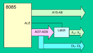
• The address bus has 8 signal lines A8 – A15 which are unidirectional.
• The other 8 address bits are multiplexed (time shared) with the 8 data bits.
– So, the bits AD0 – AD7 are bi-directional and serve as A0 – A7 and D0 – D7 at the same time.
• During the execution of the instruction, these lines carry the address bits during the early part, then during the late parts of the execution, they carry the 8 data bits.
– In order to separate the address from the data, we can use a latch to save the value before the function of the bits changes.
Demultiplexing AD7-AD0
– From the above description, it becomes obvious that the AD7– AD0 lines are serving a dual purpose and that they need to be demultiplexed to get all the information.
– The high order bits of the address remain on the bus for three clock periods. However, the low order bits remain for only one clock period and they would be lost if they are not saved externally. Also, notice that the low order bits of the address disappear when they are needed most.
– To make sure we have the entire address for the full three clock cycles, we will use an external latch to save the value of AD7– AD0 when it is carrying the address bits. We use the ALE signal to enable this latch.
– Given that ALE operates as a pulse during T1, we will be able to latch the address. Then when ALE goes low, the address is saved and the AD7– AD0 lines can be used for their purpose as the bi-directional data lines.
Demultiplexing the Bus AD7 – AD0
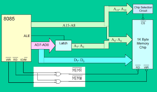
• The high order address is placed on the address bus and hold for 3 clk periods,
• The low order address is lost after the first clk period, this address needs to be hold however we need to use latch
• The address AD7 – AD0 is connected as inputs to the latch 74LS373.
• The ALE signal is connected to the enable (G) pin of the latch and the OC – Output control – of the latch is grounded.
The Overall Picture
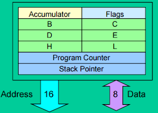
Draw 8085 register based structure microprocessor & define the registers.
Assembly language CSE Microcomputer Microcontroller. MicroprocessorLogic unit (ALU):
This register used to store 8-bit data and in performing arithmetic and logical
Operations:
Flag register:
The ALU includes five flip-flops that are set or reset according to data conditions in the
accumulator and other registers. There are five different types of data conditions:
1. Zero flag
2. Carry flag
3. Sign flag
4. Parity flag
5. Auxiliary carry flag.
Stack Pointer:
The stack pointer is a 16-bit register used as a memory pointer, it points to a memory
location in read or write memory.
Program Counter:
This 16-bit register is a memory pointer. Memory location has 16-bit address and
that is why this a 16-bit register.
Subscribe to:
Comments (Atom)


